Success Cases
Successful Projects
A successful project is every project that reaches specifications within cost and schedule constraints. Chipus’ team interacts closely with the customer and proactively provides solutions that helps the project become successful.
Chipus has successfully delivered designs for customers in South and North America, Europe and Asia.
Chipus' Success Stories
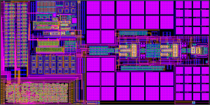
PMIC for IoT
This PMIC is able to deal with 1.8A when active and consume only 350nA when in sleep mode. It contains 3 DC/DCs (bucks and boost), 1.1A battery charger, LED drivers, load switches and more. The input voltage may go as high as 20V. It is compatible with USB charging interface and communication uses two-wire interface.
Chipus' team was responsible for specification, design and production test.
Chipus' team was responsible for specification, design and production test.
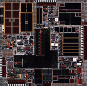
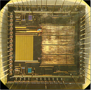
Magnetic Sensor ASIC
This ASIC was designed to develop an innovative magnetic sensor IP into a product. The design was entirely made to ensure the best of this new technology was used in silicon. The ASIC features a custom AFE with sensor biasing, an ULP capless PMU, LED drivers and eFuses (also designed at Chipus).
Chipus' team was responsible for specification, design and production test.
Chipus' team was responsible for specification, design and production test.
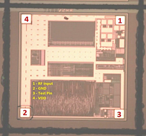
RFID ASICs
Chipus was responsible for the design of 3 RFID ASICs compatible with EPC Gen 2 and GB (Chinese) protocols. The RF front-end was designed at Chipus to match the stardards while the RTL of the baseband and NVM were licensed from partners.
Chipus' team was responsible for specification, design and production test.
Chipus' team was responsible for specification, design and production test.
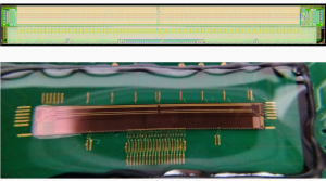
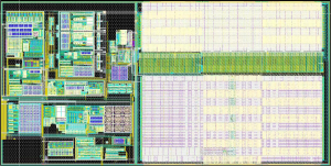
10 bit 300MSPS Pipeline ADC
Chipus team was in charge of working on a 10 bit 300MSPS pipeline ADC. The nature of the internal signals demanded the design of high bandwidth amplifiers to ensure enough settling time. Layout was also a challenge as parasitic had to be minimized not to impact on the bandwidth.
Chipus' team was responsible for the design of the IP and layout.
Chipus' team was responsible for the design of the IP and layout.
Temperature Sensor IP
Chipus was hired to develop a temperature sensor IP with digital readout for integration in SoC. In advanced nodes, design must take into account variations and design verification must be thorough. Layout dependent effects (LDE) are very pronounced and post-layout verification is essential to ensure accuracy.
Chipus' team was responsible for the design of the IP and layout.
Chipus' team was responsible for the design of the IP and layout.
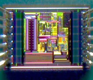
Camera readout ASIC
Chipus was hired to implement this readout ASIC. The client developed the analog section and Chipus was responsible for developing specification document, RTL, functional verification, DFT insertion, digital backend (integrating the IP from customer), tapeout and bring up.
Chipus' team was responsible for the ASIC design, dealing with foundry/bump house and bring up.
Chipus' team was responsible for the ASIC design, dealing with foundry/bump house and bring up.
36V 3A Buck DC/DC converter ASIC
This Buck DC/DC converter ASIC is capable of delivering 3A from unregulated 36V supply. Power devices were implemented using NMOS in both high side and low side. It features PWM and PFM operation modes with various switching frequencies implemented in internal oscillators. The ASIC also features all builti-in ultra low power references.
Chipus' team was responsible for the ASIC design and test.
Chipus' team was responsible for the ASIC design and test.
Low offset precision amplifier
This low offset amplifier was requested for analog signal processing. The signal bandwidth was not small enough to allow the use of chopping. Chipus chose a continuous time auto-zero architecture. In this design, all compensation capacitors are integrated.
Chipus' team was responsible for the development of the IP.
Chipus' team was responsible for the development of the IP.
Proprietary uC with analog peripherals
This ASIC contains an 8 bit proprietary uC with several integrated peripherals such as SRAM, watchdog, timers and serial interface. It also features several analog functions such as a 30V power management unit, capacitive touch sensors interface and a 10 bit SAR ADC.
Chipus' team was responsible for the specifications, design, qualification and logistics for package.
Chipus' team was responsible for the specifications, design, qualification and logistics for package.
300mA buck DC/DC converter IP
This Buck DC/DC converter IP can deliver 300mA from unregulated 5V supply. The output voltage is configurable from 1.0V to 3.3V through digital interface. Power devices are implemented in the IP and it features PWM and PFM operation modes with 3MHz switching frequency.
Chipus team was in charger of porting existing IP from SilTerra 0.18um BCD to TSMC 0.18um BCD
Chipus team was in charger of porting existing IP from SilTerra 0.18um BCD to TSMC 0.18um BCD
CONTACT US
Need Help? Get in touch with us!
- Email us here
- +55 48 3365 2740
- USA Office
5201 Great America Parkway Suite 320 Santa Clara, CA 95054 - Design Center
Rua Emilio Blum, 131 • Sala 1006 Florianópolis • SC
88020-010 • Brazil